X-Ray Photoelectron Spectroscopy (XPS) explained…
As the demand for high performance materials increases, so does the importance of surface engineering. The material’s surface is the point of interaction with the external environment and other materials, therefore many of the problems associated with modern materials can be solved only by understanding the physical and chemical interactions that occur at the surface, or at the interfaces of a material’s layers. The surface will influence such factors as corrosion rates, catalytic activity, adhesive properties, wettability, contact potential and failure mechanisms.
Surface modification can be used to alter or improve these characteristics, and so surface analysis is used to understand surface chemistry of a material, and investigate the efficacy of surface engineering. From non-stick cookware coatings to thin-film electronics and bio-active surfaces, X-ray photoelectron spectroscopy is one of the standard tools for surface characterization.

X-ray photoelectron spectroscopy (XPS), also known as electron spectroscopy for chemical analysis (ESCA), is a technique for analyzing the surface chemistry of a material. XPS can measure the elemental composition, empirical formula, chemical state and electronic state of the elements within a material. XPS spectra are obtained by irradiating a solid surface with a beam of X-rays while simultaneously measuring the kinetic energy and electrons that are emitted from the top 1-10 nm of the material being analyzed. A photoelectron spectrum is recorded by counting ejected electrons over a range of electron kinetic energies. Peaks appear in the spectrum from atoms emitting electrons of a particular characteristic energy. The energies and intensities of the photoelectron peaks enable identification and quantification of all surface elements (except hydrogen).
Surface Characterization
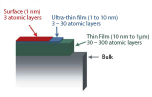
A surface layer is defined as being up to three atomic layers thick (~1 nm), depending upon the material. Layers up to approximately 10 nm are considered ultra-thin films, and layers up to approximately 1 μm are thin films. The remainder of the solid is referred to as bulk material. This terminology is not definitive however, and the distinction between the layer types can vary depending upon the material and its application.

The surface represents a discontinuity between one phase and another and, therefore, the physical and chemical properties of the surface are different from those of the bulk material. These differences affect the topmost atomic layer of the material to a large extent. In the bulk of the material, an atom is surrounded on all sides in a regular manner by atoms composing that material. Because a surface atom is not surrounded by atoms on all sides, it has bonding potential, which makes the surface atom more reactive than atoms in the bulk.
Surface Properties
Common properties and processes as a function of the depth or thickness that is important for the specific properties or processes. Surface analysis contributes to the understanding for each of these areas:
|
|
Downloads............
Application Notes
XPS is useful for investigating almost all surface problems. Below are examples of how XPS data can be used to solve problems with existing surface interactions, or to investigate new materials.
Click on a link to download the corresponding application note PDF.
Biological
- Analysis of a Wound Dressing
- Characterization of Chemical Gradients and Antibody Immobilization Using XPS and ARXPS
- XPS Surface Characterization of Disposable Laboratory Gloves and the Transfer of Glove Components to Other Surfaces
- Analyzing Contact Lens Samples
Catalysis
- Investigating the Oxidation of a Cobalt-based Catalyst Using X-ray Photoelectron Spectroscopy
- Surface Chemical-State Analysis of Metal Oxide Catalysts
Defect Analysis
- Fast, Effective XPS Point Analysis of Metal Components
- Adhesion Failure Analysis
- Mapping of the Work Function of a Damaged Solar Cell
- XPS Analysis of a Surface Contamination on a Steel Sample
- XPS Analysis of Defects on a Painted Surface
- XPS Surface Characterization of Disposable Laboratory Gloves and the Transfer of Glove Components to Other Surfaces
Energy
- Analysis of Electrode Materials for Lithium Ion Batteries
- Analysis of Solid Oxide Fuel Cell Material with XPS
- Compositional XPS Analysis of a Cu(In,Ga)Se2 Solar Cell
- Characterization of Low-Emissivity Glass Coatings using X-ray Photoelectron Spectroscopy
- Characterization of Thin Gold Layers on Steel Separators for Fuel Cell Applications
- Mapping of the Work Function of a Damaged Solar Cell
- Video: Analyzing surface chemistry of the battery and energy storage materials with XPS techniques
Glass Coatings
Microelectronics
- Composition, coverage and band gap analysis of ALD-grown ultra thin films
- Compositional XPS Analysis of a Cu(In,Ga)Se2 Solar Cell
- Analysis of a Dry Film Photo-Resist
- Multitechnique Surface Characterization of Organic LED Material
- Analysis of Solid Oxide Fuel Cell Material with XPS
- XPS Analysis of a Hard Disk Platter by Rapid Depth Profiling
- XPS Characterization of ‘Click’ Surface Chemistry
- XPS Characterization of Membrane Electrode Assembly from Proton Exchange Fuel Cell
- Understanding the chemical and electronic properties of OLED materials
- Identifying structures on a plasma-modified polymer surface
- Confirming the layer structure of an organic FET device
- Video: High performance multi-technique XPS System for semiconductor device analysis
Multi-technique
- Advantages of Coincident XPS-Raman in the Analysis of Mineral Oxides Species
- Composition, coverage and band gap analysis of ALD-grown ultra thin films
Oxides & Metals
- Advantages of Coincident XPS-Raman in the Analysis of Mineral Oxides Species
- Hydrogen and Chemical Quantification of an Organic Coating
- Cleaning Metal Oxides Using Argon Cluster Ions to Prevent Surface Modification
- Investigating the Oxidation of a Cobalt-based Catalyst Using X-ray Photoelectron Spectroscopy
- Spectroscopic Analysis of Solid Oxide Fuel Cell Material with XPS
- XPS Analysis of a Surface Contamination on a Steel Sample
- XPS Analysis of Stainless Steel Surfaces
- XPS Identification of Stains on Split Steel Bearings
Polymers
- Identifying structures on a plasma-modified polymer surface
- Chemical State Mapping of Polymers
- Using X-ray Photoelectron Spectroscopy to Investigate the Surface Treatment of Fabrics
- XPS Analysis of a Dry Film Photo-Resist
Routine Analysis
- XPS Analysis of Stainless Steel Surfaces
- XPS Identification of Stains on Split Steel Bearings
- Compositional XPS Analysis of a Cu(In,Ga)Se2 Solar Cell
- Mapping of the Work Function of a Damaged Solar Cell
- XPS Characterization of Thin Gold Layers on Steel Separators for Fuel Cell Applications
- The Karlsruhe micro nose, KAMINA
- Using X-ray Photoelectron Spectroscopy to Investigate the Surface Treatment of Fabrics
- XPS Analysis of a Hard Disk Platter by Rapid Depth Profiling
- XPS Characterization of ‘Click’ Surface Chemistry
- Fast, Effective XPS Point Analysis of Metal Components


